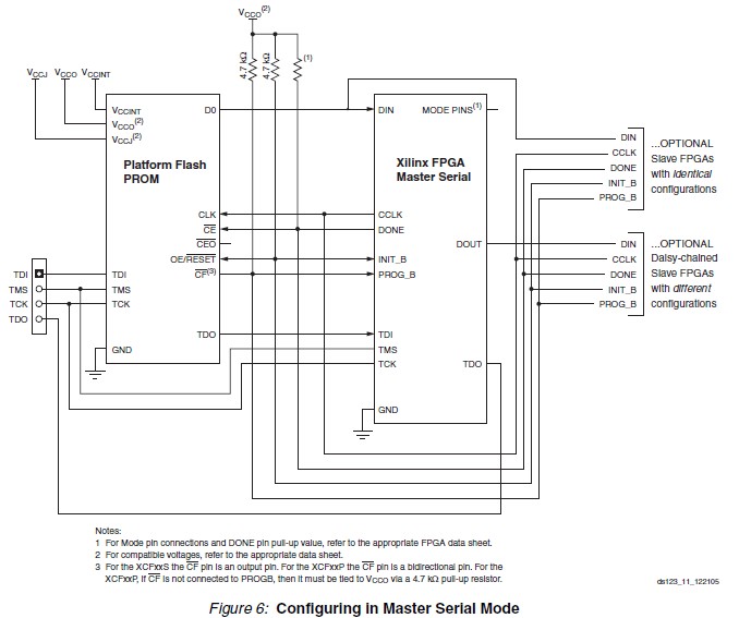
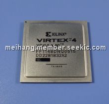
Product Summary
The XC4VLX80 is the newest generation FPGA from Xilinx.The XC4VLX80 belongs to one of the Virtex-4 FPGAs family. Virtex-4 devices are produced on a state-of-the-art 90-nm copper process, using 300 mm (12 inch) wafer technology. Combining a wide variety of flexible features, the XC4VLX80 enhances programmable logic design capabilities and is a powerful alternative to ASIC technology.
Parametrics
Absolute maximum ratings: (1)VCCINT, Internal supply voltage relative to GND: –0.5 to 1.32 V; (2)VCCAUX, Auxiliary supply voltage relative to GND: –0.5 to 3.0 V; (3)VCCO, Output drivers supply voltage relative to GND: –0.5 to 3.75 V; (4)VBATT, Key memory battery backup supply: –0.5 to 4.05 V; (5)VREF, Input reference voltage: –0.3 to 3.75 V; (6)VIN: I/O input voltage relative to GND(all user and dedicated I/Os):–0.75 to 4.05 V; I/O input voltage relative to GND (restricted to maximum of 100 user I/Os)(3,4): –0.95 to 4.4v(Commercial Temperature), –0.85 to 4.3v(Industrial Temperature); 2.5V or below I/O input voltage relative to GND(user and dedicated I/Os):–0.75 to VCCO +0.5 V; (7)IIN, Current applied to an I/O pin, powered or unpowered: ±100 mA; Total current applied to all I/O pins, powered or unpowered: ±200 mA; (8)VTS:Voltage applied to 3-state 3.3V output(all user and dedicated I/Os):–0.75 to 4.05 V;Voltage applied to 3-state 3.3V output(restricted to maximum of 100 user I/Os):–0.95 to 4.4v(Commercial Temperature); –0.85 to 4.3v(Industrial Temperature); 2.5V or below I/O input voltage relative to GND(user and dedicated I/Os):–0.75 to VCCO +0.5 V; (9)AVCCAUXRX, Receive auxiliary supply voltage relative to analog ground, GNDA(RocketIO pins):–0.5 to 1.32 V; (10)AVCCAUXTX, Transmit auxiliary supply voltage relative to analog ground, GNDA(RocketIO pins):–0.5 to 1.32 V; (11)AVCCAUXMGT, Management auxiliary supply voltage relative to analog ground, GNDA(RocketIO pins):–0.5 to 3.0 V; (12)VTRX, Terminal receive supply voltage relative to GND: –0.5 to 3.0 V; (13)VTTX, Terminal transmit supply voltage relative to GND: –0.5 to 1.65 V; (14)TSTG, Storage temperature (ambient): –65 to 150 °C; (15)TSOL, Maximum soldering temperature(2): +220 °C; (16)TJ, Maximum junction temperature:+125 °C.
Features
Features:(1)high-performance logic applications solution;(2)Xesium clock technology;(3)XtremeDSP slice;(4)smart RAM memory hierarchy;(5)selectIO technology;(6)flexible logic resources;(7)built-in system monitor (voltage/temp. measurement);(8)10-bit, 200kSPS A/D converter (ADC);(9)secure chip AES bitstream encryption;(10)90-nm copper CMOS process;(11)1.2V core voltage;(12)flip-chip packaging.
Diagrams

| Image | Part No | Mfg | Description |  |
Pricing (USD) |
Quantity | ||||||
|---|---|---|---|---|---|---|---|---|---|---|---|---|
 |
 XC4VLX80 |
 Other |
 |
 Data Sheet |
 Negotiable |
|
||||||
 |
 XC4VLX80-10FF1148I |
 |
 IC FPGA VIRTEX-4LX 1148FFBGA |
 Data Sheet |

|
|
||||||
 |
 XC4VLX80-11FFG1148C |
 |
 IC FPGA VIRTEX-4 LX 80K 1148FBGA |
 Data Sheet |

|
|
||||||
 |
 XC4VLX80-10FFG1148C |
 |
 IC FPGA VIRTEX-4 80K 1148-FBGA |
 Data Sheet |

|
|
||||||
 |
 XC4VLX80-10FFG1148I |
 |
 IC FPGA VIRTEX-4 LX 80K 1148FBGA |
 Data Sheet |

|
|
||||||
 |
 XC4VLX80-11FF1148I |
 |
 IC FPGA VIRTEX-4LX 1148FFBGA |
 Data Sheet |

|
|
||||||
 |
 XC4VLX80-11FFG1148I |
 |
 IC FPGA VIRTEX-4 LX 80K 1148FBGA |
 Data Sheet |

|
|
||||||
 |
 XC4VLX80-12FFG1148C |
 |
 IC FPGA VIRTEX-4 LX 80K 1148FBGA |
 Data Sheet |

|
|
||||||
 (China (Mainland))


