(China (Mainland))

Product Summary
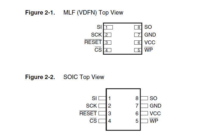
To provide optimal flexibility, the memory array of the AT45DB081D-SU is divided into three levels of granularity comprising of sectors, blocks, and pages. The "Memory Architecture Diagram" illustrates the breakdown of each level and details the number of pages per sector and block. All program operations to the AT45DB081D-SU occur on a page by page basis. The erase operations can be performed at the chip, sector, block or page level.
Parametrics
AT45DB081D-SU absolute maximum ratings: (1)Temperature under Bias: -55℃ to +125℃; (2)Temperature under Bias: -55℃to +125℃; (3)All Input Voltages (except VCC but including NC pins) with Respect to Ground: -0.6V to +6.25V; (4)All Output Voltages with Respect to Ground: -0.6V to VCC + 0.6V
Features
AT45DB081D-SU features: (1)Single 2.5V or 2.7V to 3.6V Supply; (2)RapidS Serial Interface: 66MHz Maximum Clock Frequency; (3)Flexible Erase Options: Page Erase (256-Bytes), Block Erase (2-Kbytes), Sector Erase (64-Kbytes), Chip Erase (8Mbits); (4)Two SRAM Data Buffers (256-/264-Bytes); (5)Continuous Read Capability through Entire Array; (6)Low-power Dissipation; (7)Sector Lockdown for Secure Code and Data Storage; (8)JEDEC Standard Manufacturer and Device ID Read; (9)100,000 Program/Erase Cycles Per Page Minimum; (10)Data Retention–20 Years; (11)Industrial Temperature Range; (12)Green (Pb/Halide-free/RoHS Compliant) Packaging Options.
Diagrams
| Image | Part No | Mfg | Description |  |
Pricing (USD) |
Quantity | ||||||||||||
|---|---|---|---|---|---|---|---|---|---|---|---|---|---|---|---|---|---|---|
 |
 AT45DB081D-SU |
Atmel |
Flash 8MB Serial Ind. Temp |
Data Sheet |
|
|
||||||||||||
|
AT45DB081D-SU-2.5 |
Atmel |
Flash 8MB SERIAL 2.5V - IND TEMP |
Data Sheet |
|
|
||||||||||||